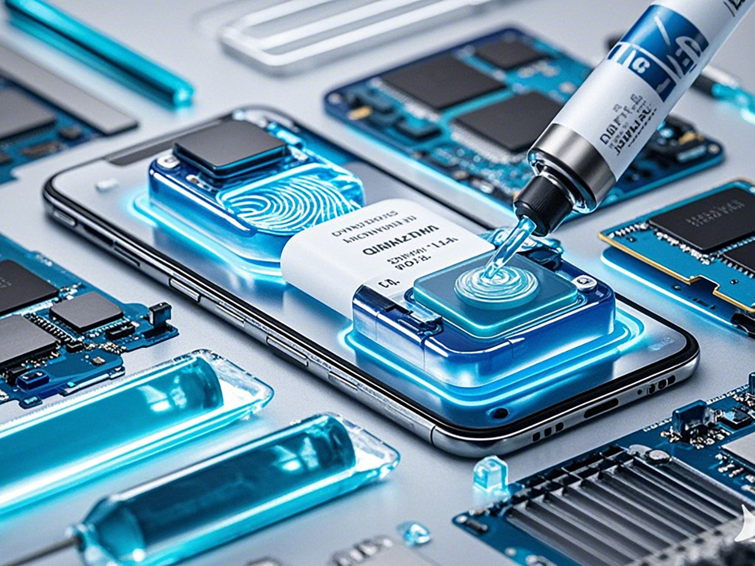
Electronic semiconductor
Mar 14,2025

1、Transparent conductive electrode
● Core material of display device
With high transmittance (80%-90%) and low resistivity (10⁻⁴ to 10⁻³ Ω·cm), ITO films serve as essential transparent electrode materials for LCD, OLED, and plasma displays, supporting high-resolution visuals and rapid responsiveness.
Touch screen technology: ITO film prepared by magnetron sputtering process is the conductive layer of capacitive touch screen to ensure touch sensitivity and anti-interference.
● Intelligent device integration
ITO film is used as a transparent circuit substrate in wearable devices and flexible electronics, supporting thin and light design and suitable for emerging scenarios such as folding screen mobile phones and flexible sensors.
2、Photovoltaic and energy devices
● Conductive layer of solar cell
ITO serves as the transparent conductive layer in heterojunction solar cells, enhancing photoelectric conversion efficiency by maximizing the effectiveness of carrier collection. Its doping effect (SnO₂ increases the carrier concentration) significantly reduces the resistance loss.
In perovskite solar cells, ITO films facilitate the efficient transport of photo-generated carriers. Their wide bandgap properties (3.5-4.3 eV) help minimize light absorption losses, enhancing overall energy conversion efficiency in these advanced photovoltaic technologies.
● High frequency power device
The high mobility, contributed by the indium component, and the cubic crystal structure of ITO make it an ideal choice for high-frequency electronic devices, such as RF modules in communication base stations, ensuring stable signal transmission.
3、Semiconductor functional materials
● Sensor technology
The catalytic activity and gas-sensitive properties of indium oxide are used in gas sensors and photoelectric detectors. Sensitivity to specific gases (e.g., NO2, CO) can be enhanced by surface modification.
Ultraviolet detection:The wide band gap of 3.6–4.0 eV in ITO makes it highly sensitive to ultraviolet light, making it an excellent material for developing solar-blind ultraviolet detectors. This property ensures effective UV detection while preventing interference from visible light.
● Semiconductor doping and structure regulation
Advantages of Solid Solutions:ITO (Indium Tin Oxide) features a cubic solid solution formed by In₂O₃ and SnO₂. Tin doping optimizes the oxygen vacancy concentration, balancing both conductivity and transparency.
Research on alternative materials:Due to the scarcity of indium resources, alternative materials such as aluminum zinc oxide (AZO) and other target have been developed. However, indium tin oxide (ITO) still occupies the mainstream market due to its advantages in comprehensive performance.
4、Other semiconductor applications
Transparent heat reflector:The ITO thin film is used in the anti-frosting and defogging system of aircraft windshield,it can achieve rapid temperature control through electric heating.
Photoelectrocatalysis:The catalytic properties of indium oxide can enhance reaction efficiency in green energy applications, such as hydrogen production via water photolysis.
Previous:
Next:


 豫公网安备41032602000214号